Anisotropic atom motion on a row-wise antiferromagnetic surface
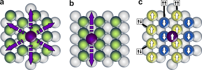
Experiments with adatoms
We have prepared extended Mn layers in fcc stacking on Re(0001)15 (see Section “Experimental details” for experimental details). The hexagonal Mn layer hosts a row-wise AFM state12,15 and in the SP-STM measurement of Fig. 2a neighboring ↑↑-rows exhibit different signal strengths16, in agreement with the DFT calculated SP-STM image shown in Fig. 2b, see Fig. S1 of the Supplemental Material for details. The symmetry allows for three equivalent rotational magnetic domains, two of which are seen in the spin-polarized (SP) STM image of Fig. 2a. The left domain exhibits a stronger magnetic contrast for this particular tip magnetization direction12.
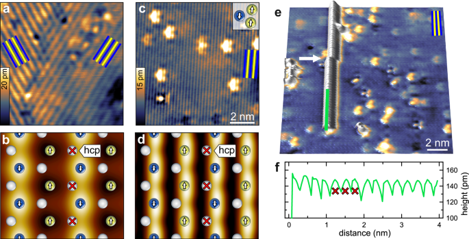
a Two rotational domains of the row-wise AFM state in fcc-Mn/Re(0001), imaged by constant current SP-STM (U = +14 mV, I = 1 nA). b Calculated SP-STM image at U = +50 mV, 3 Å above the surface based on DFT, overlaid with Mn atoms (Blue/Yellow) and surface Re atoms (Gray); adatom hcp sites are marked by red crosses. c High resolution (non-magnetic) STM image (U = +30 mV, I = 1 nA) of the ↑↑-rows with native defects reflecting the broken symmetry of the hollow sites, see inset. d DFT calculated (non-magnetic) STM image at U = +50 mV, 3 Å above the surface. e A single Co atom is imaged while it is moving to the top of the image, guided by the ↑↑-rows (slow scan direction: bottom → top, fast scan direction: left → right). f The line section shows that the Co atom is imaged with an atomic periodicity of 2.7 Å, see red crosses in panels b and d.
When the tunnel current is not spin-polarized, as in Fig. 2c, the magnetic state can be imaged as a stripe pattern of half the period, i.e. neighboring ↑↑-rows appear identical. This experimental data is nicely reproduced by our DFT-calculated STM image in Fig. 2d: Whereas the Mn atoms are equivalent, the ↑↑-rows are electronically different from the ↑↓-rows, due to the magnetic state. This means that the C3 symmetry of the system is broken, which is also reflected by the boomerang-like shape of native defects (see Fig. 2c); the defect shape is correlated with the orientation of the magnetic state (see the “Methods” section).
With a different non-magnetic tip in Fig. 2e, the Mn layer itself appears featureless, but the direction of the ↑↑-rows can still be inferred from the defect shapes. Co adatoms on fcc-Mn/Re(0001) are easily moved during standard STM imaging: in Fig. 2e a single Co atom jumps along the ↑↑-rows and is imaged again in every line and therefore appears like an atomic chain. Only once does the atom jump one atomic row to the right (see arrow in Fig. 2e). This data is reminiscent of the experiments performed by Li et al. with Ag atoms on Ag(110)3,17 and is a first hint that the magnetic state dictates the movement direction of Co atoms. The line section in Fig. 2f shows the period of the atomic lattice, indicating that only one type of hollow site is a stable position for Co, in agreement with no zigzag movement being observed. On all other positions, the residence time is too short to be detectable in this measurement. We will see in section “First-principles calculations” that the Co atoms prefer the so-called hcp hollow site above the surface Re atom, see red crosses in Fig. 2b and d.
To minimize the influence of the tip, instead of dragging the adatom along during imaging, as in Fig. 2e, in the following, we “kick” the adatoms with a voltage pulse from a stationary tip and determine the new position by subsequent imaging. The kicking is performed by a sudden voltage increase at a constant tip height above the atom, which also leads to an increased tunnel current (see inset of Fig. 3a and “Methods” section). By performing these experiments with one and the same micro-tip on different rotational domains, we can exclude a possible tip asymmetry being responsible for the movement direction. Figure 3a shows a surface area with two rotational domains like in Fig. 2a, this time imaged with vanishing spin contrast. The domain wall (DW), now visible via a reduced electron density12, is marked by a white line. We find that the Co movement initiated by kicking is always toward the upper left on the left domain and toward the top of the image on the right domain, in both cases following the ↑↑-rows of the magnetic state (Supplementary Movie 1). Examples are given in Fig. 3b and c (left domain) and Fig. 3d and e (right domain). Which of the two equivalent directions along the ↑↑-rows of a particular domain is taken, can depend on the specific micro-tip: for some tips, like the one used in Figure 3a–e, one movement direction is favored; other tips show a more symmetric distribution. Independent of the micro-tip used for kicking, we always observe a strictly one-dimensional movement of Co atoms along the ↑↑-rows, within an accuracy of one atomic lattice site. Occasionally, Co atoms that are further away from the directly kicked atom also move 1–2 lattice sites (see Fig. 3b–d), indicating a weak long-range effect. These short jumps also occur exclusively along the ↑↑-rows.
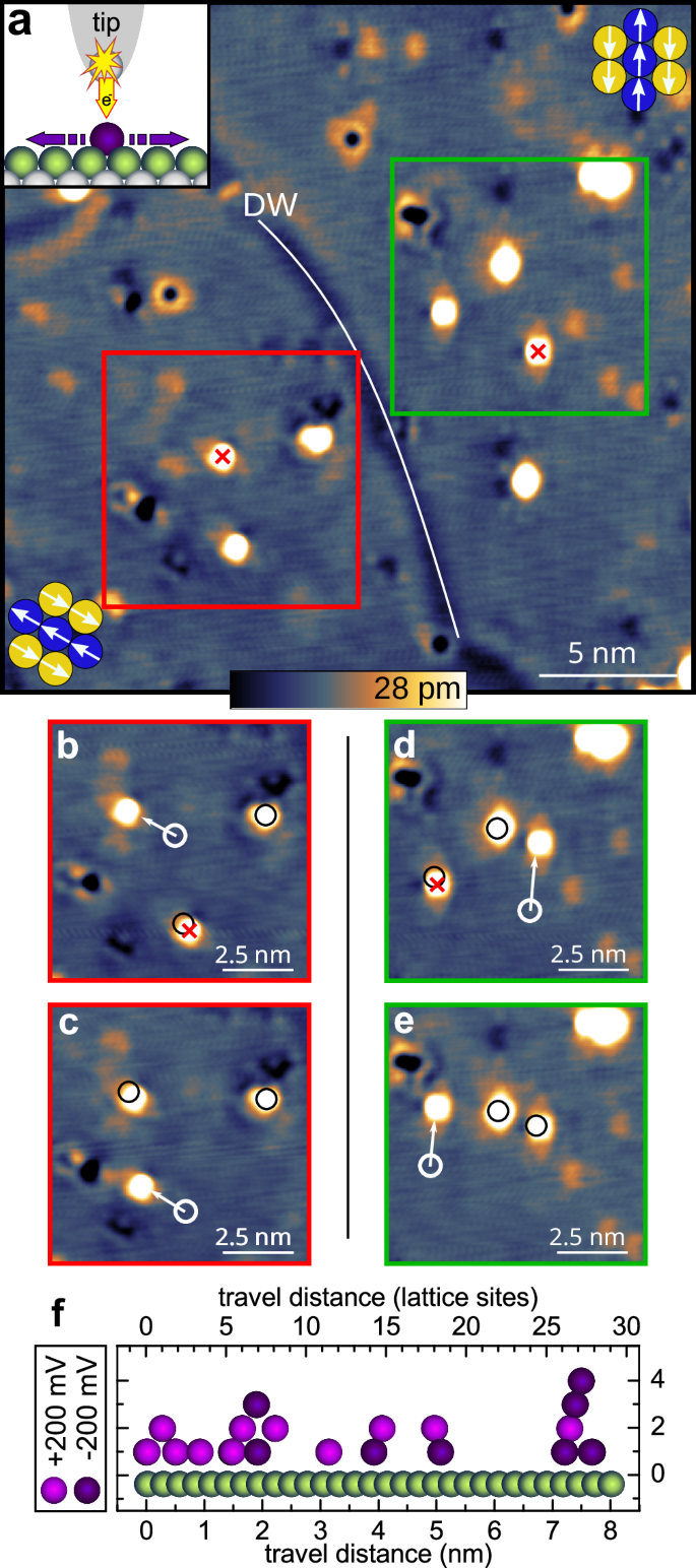
a Overview STM image of Co atoms on fcc-Mn/Re(0001) with two rotational domains; their orientation is apparent by the defect shapes and the domain wall (DW) is imaged via a reduced electron density. Kicking is performed by a sudden voltage raise at constant tip height, see inset. b The upper left Co atom has moved along the ↑↑-rows after kicking. c The bottom Co atom has moved in the same direction after kicking. d The bottom Co atom has moved along the ↑↑-rows after kicking. e The left Co atom has moved in the same direction after kicking. (All images U = +8 mV, I = 1 nA, all voltage pulses: UP = +200 mV, Δt = 1 s, tip kicking locations are marked by crosses in the previous image, previous atom positions are marked by circles.) f Kicking distances for both voltage polarities (color-coded), ∣UP∣ = 200 mV, Δt = 0.5 s.
The Co atoms are surprisingly mobile on fcc-Mn/Re(0001). Depending on the micro-tip, we find a threshold voltage for single-site jumps at a rather low voltage, in the range of 8–50 mV at I = 1 nA. In Fig. 3b–e Co atoms move 10–15 lattice sites when kicked by voltage pulses of UP = +200 mV. A further measurement series of 19 kicking events, using both voltage polarities (see also Supplemental Material) is shown in Fig. 3f: the average travel distance is similar as before and the distribution is roughly uniform with an accumulation at the far end at 7–8 nm. We observe a maximum kicking distance of about 10 nm at UP = 500 mV. A random walk-type motion of uncorrelated short jumps would lead to a normal distribution with a maximum at zero and an exponential tail1, and can therefore be ruled out. Instead, these results indicate low diffusion barriers along the ↑↑-rows and effectively low damping, allowing the Co atoms to perform long jumps18,19.
To make a more general case we repeated the above experiments with a second adatom species: Rh is in the same chemical group and thus iso-electronic to Co, but almost 75% heavier and typically non-magnetic on metal surfaces. We again use a surface area with two rotational domains to exclude tip artifacts (see Fig. 4a). We similarly find that the movement is always along the ↑↑-rows (Supplementary Movie 2), as can be seen in Fig. 4b, c (upper domain) and in Fig. 4d, e (lower domain). The Rh atoms show no spherical symmetry but instead reflect the broken C3 symmetry, like many of the native defects. In comparison, the Co shows an asymmetry in the extended electron density surrounding the atom (see Fig. 3a–e). Apparently, Rh is much less mobile than Co: at UP = +200 mV Rh atoms do not move more than one atomic site and at UP = +1 V they travel only 1.0–2.5 nm (see Fig. 4b–e). We observe a maximum travel distance of 3 nm at UP = +2 V.
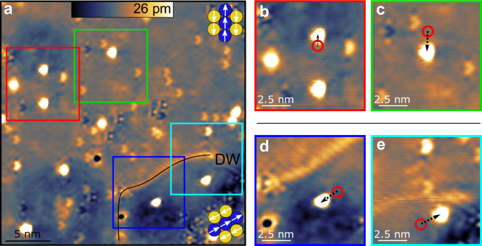
a Overview STM image of Rh atoms on fcc-Mn/Re(0001) with two rotational domains. A domain wall (DW) is marked by a black line. b–e When kicked, the Rh atoms also move according to the rotational domain state, but travel shorter distances compared to Co, despite the use of pulses with higher voltage magnitude. The electron density of native defects and also the Rh atoms are asymmetric due to the AFM state (all images U = +25 mV, I = 2 nA, UP = +1 V, Δt = 400 ms).
Attempts to kick Ir atoms with similar parameters failed, indicating that Ir is even less mobile than Rh. However, in one case we were able to initiate one-dimensional movement along the ↑↑-rows of the AFM state, by imaging at high voltages and high tunnel current (see Fig. S2 of the Supplemental Material). We thus find for Co and Rh strictly one-dimensional movement, within an accuracy of one atomic site, and for Ir some indication of the same behavior. The critical parameter to move an atom seems to be the voltage magnitude ∣UP∣. The threshold voltage is tip-dependent and element-specific with UP = 8–50 mV for Co and UP = 200–300 mV for Rh.
First-principles calculations
In order to explain the experimental observations we performed DFT calculations. We find that for the fcc-stacked Mn monolayer on Re(0001) the row-wise AFM state is energetically much more favorable (by 300 meV/Mn atom) than the ferromagnetic (FM) state. The experimental result of Fig. 2c highlights the symmetry breaking of the substrate due to the row-wise AFM state. Consequently, in the structural relaxations of fcc-Mn/Re(0001) we have also allowed for a lateral relaxation of the Mn atoms. Indeed, in addition to a relaxed Mn–Re interlayer distance, we also find a lateral shift of the Mn monolayer by ~15 pm, moving the Mn atoms of the ↑↑-rows closer to bridge sites of the substrate (see Fig. 2b and d). As a result, the induced magnetic moments of the Re surface atoms are enhanced, and the antiferromagnetic Mn–Re interaction becomes stronger (The lateral shift of the Mn layer results in a total energy gain of 18 meV/Mn atom for the row-wise AFM state. Thereby, it becomes the magnetic ground state of the system since it is lower than all spin spiral states as well as the triple-Q state15.). Note, that an even larger magnetism-driven lateral shift occurs for an Mn bilayer on Ir(111) with a row-wise AFM state as recently reported in ref. 20. For our laterally shifted lowest energy row-wise AFM state we find that the Mn magnetic moments of mMn ≈ 3.4μB point in-plane along the ↑↑-rows (Fig. 5a) due to the easy-plane magnetocrystalline anisotropy and the anisotropic symmetric exchange interaction15.
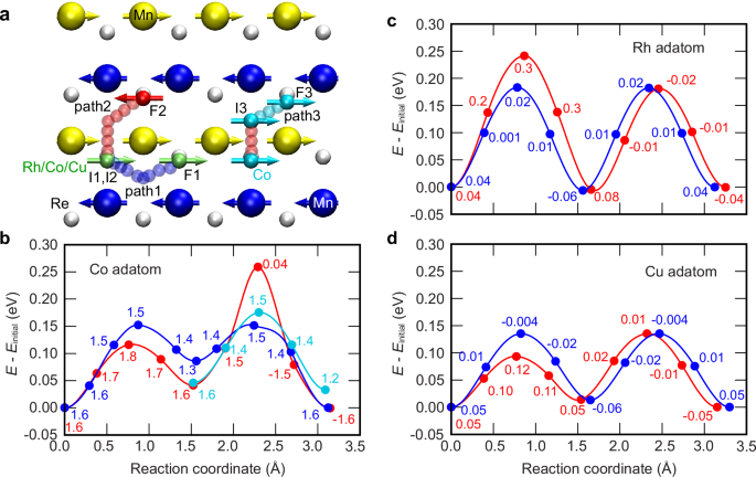
a Minimum energy path for the quasi-one-dimensional movement of Rh and Co adatoms between close-packed atomic rows of the fcc-Mn/Re(0001) surface in the row-wise AFM state obtained via DFT nudged-elastic band calculations. Yellow and blue spheres with arrows represent Mn atoms with opposite spin directions. Gray spheres denote Re surface atoms, while small green, red, and cyan spheres represent adatoms. Note that the lateral shift of the Mn layer with respect to the Re surface obtained from DFT is included in the sketch. Blue and red transparent spheres indicate the DFT calculated minimum energy paths 1 and 2, respectively, from the hcp hollow adsorption site (initial states I1 and I2) to two similar adsorption sites with opposite spin directions (final states F1 and F2). For the Co atom, the minimum energy path is also given from the initial state I3 to the final state F3 (cyan spheres, path 3). b–d Energy along the minimum energy paths 1 and 2 for Rh, Co, and Cu atoms from the initial state I1 and I2 to the final states F1 and F2 along the red and blue paths indicated in panel a, respectively. For the Co atom, the energy is also given along minimum energy path 3 from I3 to F3 (cyan symbols and line). The magnetic moment of the Rh, Co, and Cu atom is given in μB at every image along the paths.
To investigate the experimentally observed anisotropic motion of Co and Rh adatoms on this substrate we calculate via DFT the minimum energy paths and the related energy barriers for different directions of adatom movement using the climbing image nudged elastic band (NEB) method21,22 (see the “Methods” section). For both atom species the preferred adsorption site is the hcp-hollow site, and we move the adatom from the initial hcp-hollow site (I) to a final adjacent hcp-hollow site (F) via different paths (see Fig. 5a). We start our discussion with the Co adatom, which possesses an intrinsic magnetic moment of about +1.6μB and favors a parallel alignment to the Mn atoms of the substrate, see the indicated spin in the initial state of Fig. 5a. For path 1 (blue) the adatom spin points along the same direction for states I1 and F1, whereas on path 2 (red) the adatom crosses an ↑↑-row and a spin–flip is required from I2 to F2 (see Fig. 5a). We find that on both paths the adatom roughly moves via the intermediate fcc-hollow site. Our calculations for the Co adatom (Fig. 5b) show that path 1 is symmetric, with two saddle points near the ↑↓-bridge sites, resulting in an energy barrier height of ~150 meV, and one intermediate energy minimum near the fcc hollow site. Interestingly the Co adatom does not move to the center of the fcc hollow site, where an inverted moment would be expected. Instead, the magnetic moment direction does not change along the entire path 1 and only shows slight variations of its magnitude, as indicated by the numbers in Fig. 5b.
On path 2 (red) the Co adatom crosses two inequivalent bridge sites and the preferred spin directions in I2 and F2 are opposite, resulting in a more complex minimum energy path. We find that the saddle point to cross the ↑↑-bridge site of path 2 has lower energy compared to the ↑↓-bridge sites of path 1. In contrast to path 1, on path 2 the Co crosses the center of the fcc-hollow site, as the respective spin direction is favored in this case, compare intermediate minima of paths 1 and 2. The second part of path 2 exhibits a high energy barrier of ~260 meV at the ↑↓-bridge site, where the Co magnetic moment is nearly quenched (0.04μB), which results from the required spin-flip along the path and the constraint to collinear magnetic moments in our calculation14. Finally, the Co adatom arrives at F2 where it has the opposite spin direction compared to I2. With an overall barrier height of ~260 meV, path 2 is clearly unfavorable with respect to a Co movement along ↑↑-rows (path 1), consistent with our experimental observations.
To reveal the role of the Co spin–flip on the energy barrier for the path across an ↑↑-row, we have performed a minimum energy path calculation from I3 to F3 with the constraint that the Co adatom spin cannot flip (cyan spheres and line in Fig. 5a and b). We find that now the energy barrier is significantly reduced for the ↑↓-bridge site, with a Co magnetic moment of 1.5μB. The spin of the Co atom may flip after the metastable state F3 has been reached such that relaxation into the favorable state F2 is achieved. The initial state I3 of path 3 coincides with the intermediate energy minimum of path 2 (see Fig. 5a and b). Therefore, we can combine the first half of the path 1 with path 3. While this new path 3 has a significantly lower energy barrier compared to path 2, where the spin flip occurred near the bridge site, the lowest energy path for the Co adatom remains path 1, where the Co adatom effectively moves parallel to the ↑↑-row, in agreement with the experiment.
Next, we study the movement of a Rh adatom along paths 1 and 2 (see also Supplementary Fig. 3). The induced magnetic moment in the hollow sites is on the order of only 0.04–0.08μB, (see Fig. 5c). The ↑↓-bridge site energy barriers of the symmetric path 1 are lower than the ↑↑-bridge site on path 2. The different magnetic moments of the Rh adatom in the different bridge sites, i.e. 0.02μB versus 0.3μB at ↑↓- and ↑↑-bridge sites, respectively, suggest that a high induced moment is unfavorable and leads to the increased energy barrier. In contrast to the case of the Co adatom, where the reduction of the magnetic moment leads to an increase of the energy barrier, in the case of Rh a large magnetic moment results in an increased barrier. Based on the local density of states (LDOS, see Supplementary Fig. 4), we attribute this effect to the spin-dependent hybridization of the adatoms with the Mn surface atoms which is distinctively different for Rh and Co. For the Rh atom, the increased spin moment at the ↑↑-bridge site is connected to an energetically unfavorable enhancement of the LDOS close to the Fermi energy. Despite this opposite behavior, Co and Rh adatoms both have path 1 as the lowest energy path, as also seen in the experiments of Figs. 3 and 4. Note, that for the Rh atom motion, the magnetism-induced lateral shift observed for the Mn layer on Re(0001) plays a key role. NEB calculations for an unshifted Mn layer lead to almost isotropic minimum energy paths (see Supplementary Fig. 5).
To facilitate a more complete understanding of magnetism-induced anisotropic motion we also discuss our result for a Cu adatom (see Fig. 5d). The induced magnetic moment of the Cu adatom is on a similar scale as that of the Rh atom. However, in contrast to the case of Rh, an increased Cu magnetic moment at the ↑↑-bridge site is accompanied by a lower energy barrier on path 2 as compared to the energy barrier at the ↑↓-bridge along path 1. Due to its fully occupied 3d bands, Cu exhibits only a small LDOS at the Fermi energy. Therefore, the hybridization occurs dominantly between the occupied 3d-bands of Cu and Mn which can explain the different behavior (Supplementary Fig. 4). In consequence, the predicted motion of the Cu adatom is still anisotropic, but in contrast to Co and Rh the preference is along the two ↑↓-row directions of the row-wise AFM state, allowing for two-dimensional diffusion.
link



.jpg)